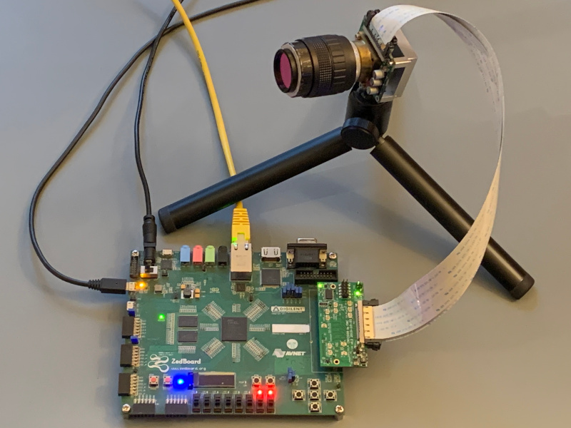
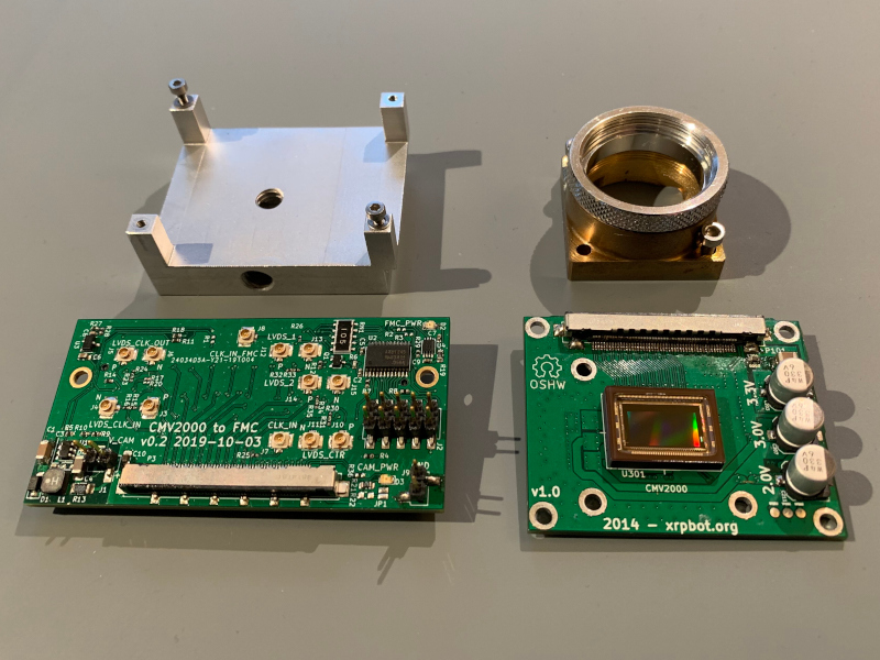
This adapter kit allows connecting an AMS CMV2000 image sensor to a ZedBoard (and probably other FPGA devboards) via the FPGA Mezzanine Card (FMC) connector.
The CMV2000 is a high-speed image sensor intended for machine vision applications (2 megapixels, 340 fps). While relatively expensive, it is one of the few mid-range image sensors where reasonably complete documentation is freely available (without NDA) from the manufacturer.
The hardware is split in two PCBs, connected by two high speed flat flex cables. The first board contains the sensor, the second board connects to the FMC port on the ZedBoard.
The sensor is powered by the ZedBoard, using the 12 V supply provided on the FMC connector. Level shifters are used to translate all single-ended signals from the FPGA I/O voltage to the 3.3 V used by the sensor.
The FMC board contains integrated 1k probes for some of the high-speed differential signals. Additionally, a pin header allows probing the low-speed single-ended signals.
For space reasons, the 1k probes use U.FL connectors for the connection to the oscilloscope. The U.FL connectors have a very limited number of mating cycles and the number of connections must therefore be kept to a minimum. Note that a 1k probe generally requires a termination (typically 50 Ω) at the oscilloscope; with a high-impedance input, results will be very poor. If the 1k probes are not required, the connectors and the corresponding resistors can simply be left unpopulated.
See pinmap.txt for a list of connections from FPGA package pins to camera pins.
Note that this repository uses submodules.
The FMC PCB is designed to be produced with 4 layers using the JLCPCB JLC2313 stackup. (0.1 mm prepreg, εr = 4.05 between the outer and inner layer.)
Using the JLCPCB impedance calculator, the following trace parameters were obtained:
100 Ω differential: 4.00 mil (102 µm) trace width / 5.00 mil (127 µm) space
50 Ω single-ended: 5.78 mil (147 µm) trace width
These results were cross-checked using Maarten Baerts AlterPCB TLineSim tool. In addition, the influence of ground pour on the signal layer was investigated (using the "Coplanar Waveguide" geometry). A distance of >= 200 µm between the edge of the signal trace and ground seems to have little effect on the impedance.
JLC multilayer: min. via drill: 0.2 mm, min. via diameter: 0.45 mm
-
Sensor board: The 3.0 V rail is generated with an LDO (U202) from the 3.3 V rail. However, this drop is too low for the LDO to properly operate. On the physical board, this is fixed with a bodge wire connecting the input of U202 to the 5.0 V rail instead. However, this fix is not contained in the schematic or layout.
-
After the sensor board PCB was produced, we found out that the intended 31-pin connector (P102) was no longer available. Thus, a 41-pin connector had to be bodged on (sacrificing the I2C EEPROM). This change is not documented in the schematic. However, when the current version of the FMC board was designed, it was adapted to the situation and uses a 41-pin connector. The end result is that the boards, as found in this repository, are incompatible: the sensor board uses a 51-pin and a 31-pin connector, while the FMC board uses a 51-pin and a 41-pin connector.

