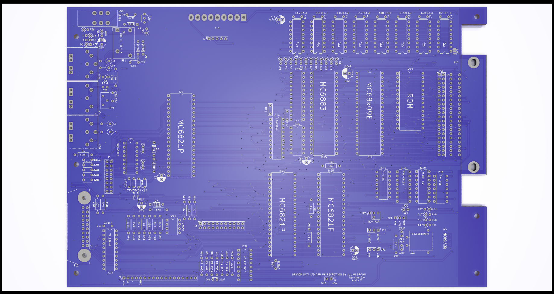
This project started as a recreation of the SA2120 CPU Mainboard for the 1982 Dragon Data Dragon 32
Everything (excluding modifications) is taken from the SA2120 schematics. Where this version changes is that the options to use banks of 16K DRAM is gone, you must use 64K DRAMs, with it goes all the extra circuitry for configuring the memory for different types of chip.
The ROM is now a single 27C256 eprom with an option to switch between two images using JP6 or to allow the rom to be automatically selected from the PIA.
A second ROM selection jumper is available at JP3 to be used when a 27C512 is fitted. This swaps the value to A15 between high and low. When a 27C256 is fitted this must be set low.
Hidden on the back of the board is a solder pad jumper (JP7) that also needs setting to handle a 27C256 or 27C512. Bridging pad 1 sets pin 22 of the rom to ground, using pad 3 sets the pin to use the ROM select signal shared with pin 20. When a 27C512 is fitted this must be set to pad 1.
The video circuits have been isolated from the rest of the board to improve output quality.
A second (internal) cartridge port has been added, by way of a 2x20 header, along with an additional +5V/Gnd pickup point for further internal expansion.
An optional 256K banking solution is incorporated using the design for Stewart Orchard's upgrade board and GAL design. https://gitlab.com/sorchard001/dragon-256k-banker-board
In the current state (3.0) none of the board is tested. This is purely experimental although the schematics have been tested with the previous rev 2 board and are largely unchanged.
The two joystick ports provide a second fire button capability wired to consecutive keyboard rows, as per the Tandy CoCo. Unless a two button joystick is used this make no difference to the operation of the computer. It also requires the use of 6-pin DIN sockets, these are pin compatible with the 5-pin originals so a regular single button joystick can still be used.
The two extra buttons can also be disabled by omitting L3 and L4.
A jumper (JP2) has been introduced to bypass the logic inverter on the STROBE line. When bypassed the parallel port should operate as a communication port for DRIVEWIRE.
The board is configurable between 32k and 64k ram addressing using jumper JP1. In most scenarios there is no reason to disable the 64k option.
The upgrade to 256K needs the 4164s swapping for 41256s. The pre-bridged jumper at JP5 needs cutting. The SAM also needs to be replaced with a 74LS785. The optional components can then be fitted and should work without further alteration.
One of the possible features of the board is to support an extended version of the video circuitry to include external character ram. Adding a third PIA to the board takes a little refinement of how PIAs are interfaced. In this case the mapped memory for PIA1 is broken into 8 blocks, this first maps to the original memory space for PIA1 while the other 7 are effectively available to more registers. On this board only the first of those 7 is used (yet). This makes addresses $FF44-$FF47 map to the new PIA (referenced here as 1b).
Register A of PIA1b is control of additional functions
bit 0 controls internal or external character image generation
bit 1 controls automatic invert on bit 6 of the data bus
bit 2 is manual control of the invert signal
bit 3 controls automatic semigraphics on bit 7 of the data bus
bit 4 is manual control of the semigraphics signal
bit 5 opens the external character ram to writing
bit 6 is a clock trigger to the external character ram address
bit 7 is unused (proposed to be CoCo compatibility switch for
the keyboard)
Register B of PIA1b is used for programming the external character ram data.
The external character ram can only be programmed while the video is set to the internal character data of the 6847.
Many of the original components are simply unobtainable or just very hard (and expensive) to locate. The transistors will need modern substitutes as the BC141, BC212 and 2N2369 are all obsolete but thankfully these are fairly run-of-the-mill transistors and shouldn't cause any particular issues.
The CPU and PIAs are all fairly easy to obtain online and possibly even new (MC6821s are still made and there are lots of compatible alternatives). A and B rated components should all be usable but make sure the processor is an "09e". The Hitachi HD6309 is usable but may cause crashes in some software due to lazy coding.
As these parts become harder to find it is inevitable that replacements and redesigns will be needed. The most obvious of these is the SAM chip. In 2023 these are pretty much unobtainable without harvesting from another Dragon or CoCo. In order to be viable the SAMs functionality needs to be replicated in a modern CPLD, this opens up an opportunity to incorporate the memory paging into a single chip, further reducing complexity on the board. In order to use the ram banking the SAM already needs to be replaced with a 74LS785, some supply of these does still exist but the numbers are painfully small.
