This is a design of a development cart for the PC-FX, based almost entirely on the RP2040 microcontroller.
A 3D model of a proper case is also included in this repository.
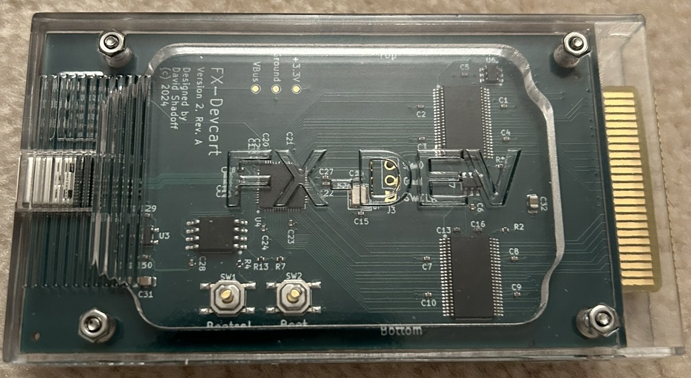
Here is a photo of a complete unit:
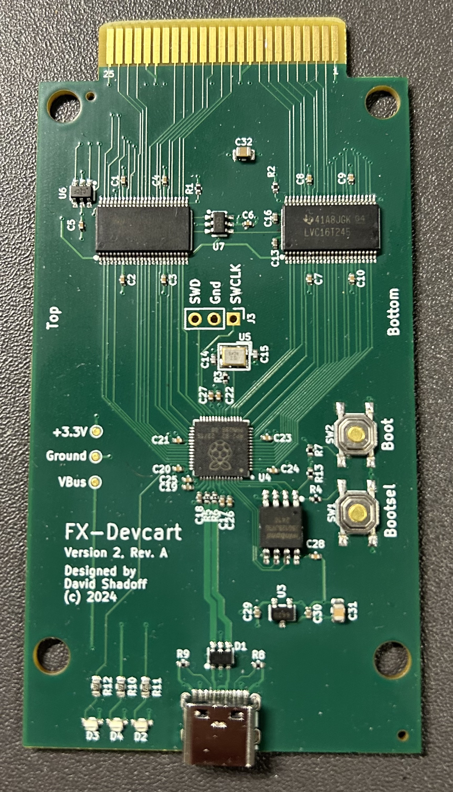
The current version is Ver2_RevB. (For the Protoype board using an Olimex RP2040-Pico30 module, please click here.)
The only changes from RevA to Rev B are related to schematic annotations, and a minor labelling update on the PC Board itself, so the picture of RevA is included here.
The basis of the FX-BMP cartridge is that it consists of 128KB of memory, and the PC-FX can actually boot from the cartridge memory under the right circumstances.
The FX-BMP memory doesn't need to be very fast - the bus access speed is cut in half when accessing the FX-BMP range of memory. Assuming that the CPU reads the data at the rising edge of /OE, this can be as slow as 174ns after /OE. (My design targets have been to keep this turnaround time below 150ns).
The RP2040 has two CPU cores, and very fast GPIO access. It seemed possible to emply one CPU core to deal with external access to the memory - emulating a SRAM bus interface - and for the other CPU core to be used as a supervisor, allowing USB commands to read/write this memory, downloading programs and preparing them to be booted from.
At 21MHz, you would expect the PC-FX to have a very fast bus access speed, however accesses to the FX-BMP port are apparently clocked at half-speed (and are only 8 bits wide).
In general, bus accesses progress through the following steps for a read cycle:
- Address lines are set up
- /CE transitions low
- /OE transitions low
- The device being queried needs to ready the data, and output it onto the data bus
- /OE transitions high
- The device being queried needs to de-assert/tri-state its outputs
- /CE transitions high
While this is the normal situation, there can also be cases where the /CE line does not return to high state before a subsequent address setup and corresponding /OE (or /WE) transition to low.
As our circuit operates at 3.3V, keep in mind that good-quality level-shifters will delay incoming signals by roughly 5ns before they appear, and an additional 10ns on the return path, reducing the available turnaround time for a read transaction.
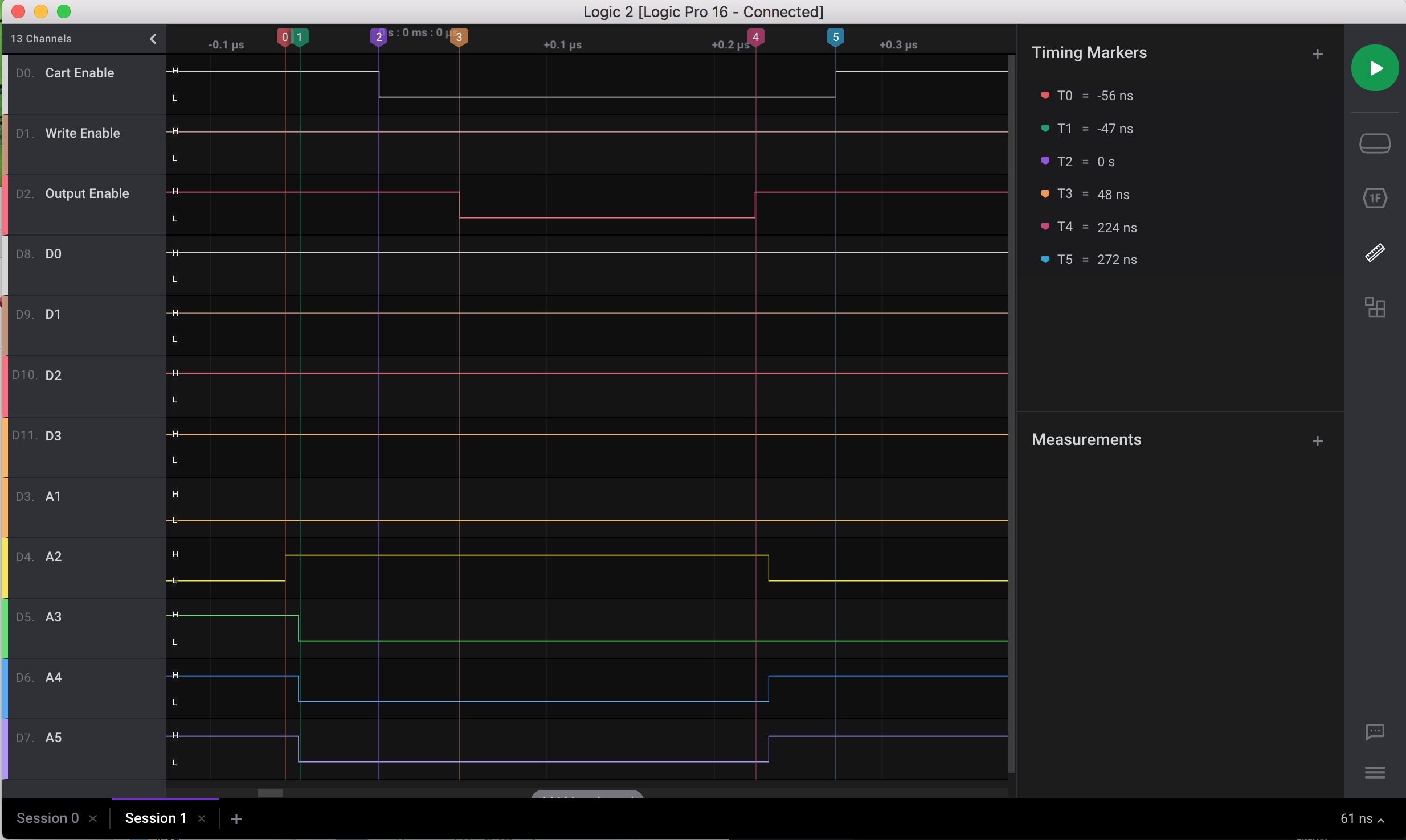
Here is a visual of the actual timing of those sequences:
In general, bus accesses progress through the following steps for a write cycle:
- Address lines are set up
- /CE transitions low
- /WE transitions low
- Data appears on the bus, to be written to the addressed device (not before /WE !)
- /WE transitions high
- In theory, the written-to device should latch data at this monment, but we can't react that fast, so we will latch earlier
- /CE transitions high
While this is the normal situation, there can also be cases where the /CE line does not returns to high state before a subsequent address setup and corresponding /WE (or /OE) transition to low.
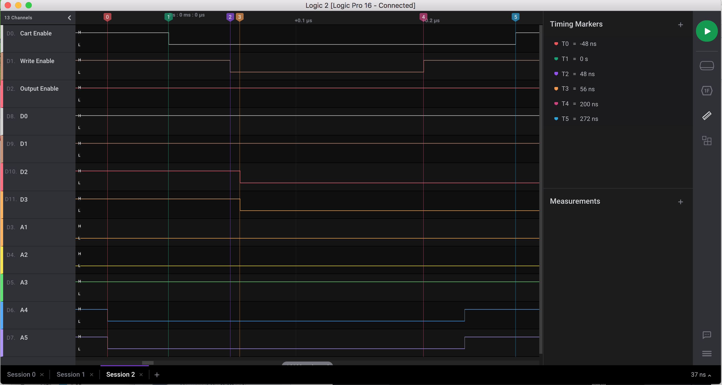
Here is a visual of the actual timing of those sequences:
My original idea was to emply PIOs to manage the bus, but there are delays in crossing between CPU and PIO (to access the CPU's memory), which hobbled performance. However, it turned out that the GPIO access functions are also very fast, enabling the RP2040 to reach the apparent required speed.
In order the reach the required speeds, the CPU is overclocked to 240MHz (the default CPU clock speed is only 125MHz, and it is only certified to 133MHz). This might at first sound a bit scary and possibly dangerous, but there are many cases of RP2040 examples out in the wild and used commonly which are clocked over 250MHz (including dricing VGA and DVI/HDMI signals), with many people finding it to work in the 400MHz range (of course, USB and Flash access break down somewhere between 250MHz and 400MHz).
| GPIO | Signal |
|---|---|
| GPIO0 | D0 |
| GPIO1 | D1 |
| GPIO2 | D2 |
| GPIO3 | D3 |
| GPIO4 | D4 |
| GPIO5 | D5 |
| GPIO6 | D6 |
| GPIO7 | D7 |
| GPIO8 | A0 |
| GPIO9 | A1 |
| GPIO10 | A2 |
| GPIO11 | A3 |
| GPIO12 | A4 |
| GPIO13 | A5 |
| GPIO14 | A6 |
| GPIO15 | A7 |
| GPIO16 | A8 |
| GPIO17 | A9 |
| GPIO18 | A10 |
| GPIO19 | A11 |
| GPIO20 | A12 |
| GPIO21 | A13 |
| GPIO22 | A14 |
| GPIO23 | A15 |
| GPIO24 | A16 |
| GPIO25 | A17 |
| GPIO26 | /CE |
| GPIO27 | /OE |
| GPIO28 | /WE |


