A DIY Powerwall is the DIY construction of a pack of battery cells to create an energy store which can be used via inverters to power electrical items in the home. Generally cells are salvaged/second hand.
Lithium batteries need to be kept at the same voltage level across a parallel pack. This is done by balancing each cell in the pack to raise or lower its voltage to match the others.
Existing balancing solutions are available in the market place, but at a relatively high cost compared to the cost of the battery bank, so this project is to design a low-cost, simple featured BMS.
Battery management system controlled by STM32G031K6 32bit microcontroller, the system has three separated units, power supply, analog digital conversion peripheral and communication unit.
Power supply is connected directly to batteries meaning that we do not need additional external power source. Power supply main part is Texas Instruments integrated circuit TPS6107x which stands as a buck/boost converter generating stable 600 mA and 3.3 V at the output. All 4.7 uF capacitors connceted to TPS6107x chip are used to give the maximum power at the output. Two 4.7 uF X7R capacitors instead of one 10uF capacitor are better solution due to less value noise generation.
The output voltage of the TPS6107x dc/dc converter can be adjusted with an external resistor divider. The typical value of the voltage at the FB pin is 500 mV. The maximum recommended value for the output voltage is 5.5 V. The current through the resistive divider should be about 100 times greater than the current into the FB pin.
The typical current into the FB pin is 0.01 µA, and the voltage across R2 is typically 500 mV. Based on those two values, the recommended value for R2 should be lower than 500 kΩ, in order to set the divider current at 1 µA or higher. Because of internal compensation circuitry, the value for this resistor should be in the range of 200 kΩ. The second parameter for choosing the inductor is the desired current ripple in the inductor. Normally, it is advisable to work with a ripple of less than 20% of the average inductor current. A smaller ripple reduces the magnetic hysteresis losses in the inductor, as well as output voltage ripple and EMI.
But in the same way, regulation time rises at load changes. Parameter f is the switching frequency and ΔIL is the ripple current in the inductor, i.e., 40% ΔIL. In this example,the desired inductor has the value of 4 µH. With this calculated value and the calculated currents, it is possible to choose a suitable inductor. In typical applications, a 4.7-µH inductance is recommended. The device has been optimized to operate with inductance values between 2.2 µH and 10 µH.
Analog to digital conversion peripheral is used to take analog values from various sources, like NTC thermistors and batteries. These sources give us battery voltage and battery temperature directly from battery connector and from the battery side. These two temperature points are added to calculate the temperature change between battery connector and battery body. ADC peripheral has an ability to generate 12 bit and 16 bit battery voltage value due to operational amplifier circuit that generates triangle shape signal making it better for microcontroller to take measurements with 4 extra bits. LMV321 is used as a main operational amplifier.
Devices are communicating in series, sharing measured values between each other. Main CPU is collecting voltage and temperature values from every unit and posting it to the PLC. System testing unit is using both half duplex and full duplex communication method. Half duplex method allows the system to communicate with another one but not in the same time whereas full duplex is making that possible.
Half and full duplex communication main elements are Texas Instruments SN65HVD10 and SN65HVD73 transreceivers circuits. ICs datasheets recommend 10 kOhms pull up resistors for receiver input line and 10 kOhms pull down resistor for transmitter line. All outputs must be protected from electrostatic discharge. ESD protection is made using 10 Ohms resistors and zener diodes with Vz = 5 V disallowing signals to have values greater than 5 V.
STM32G0 NUCLEO Reference Manual
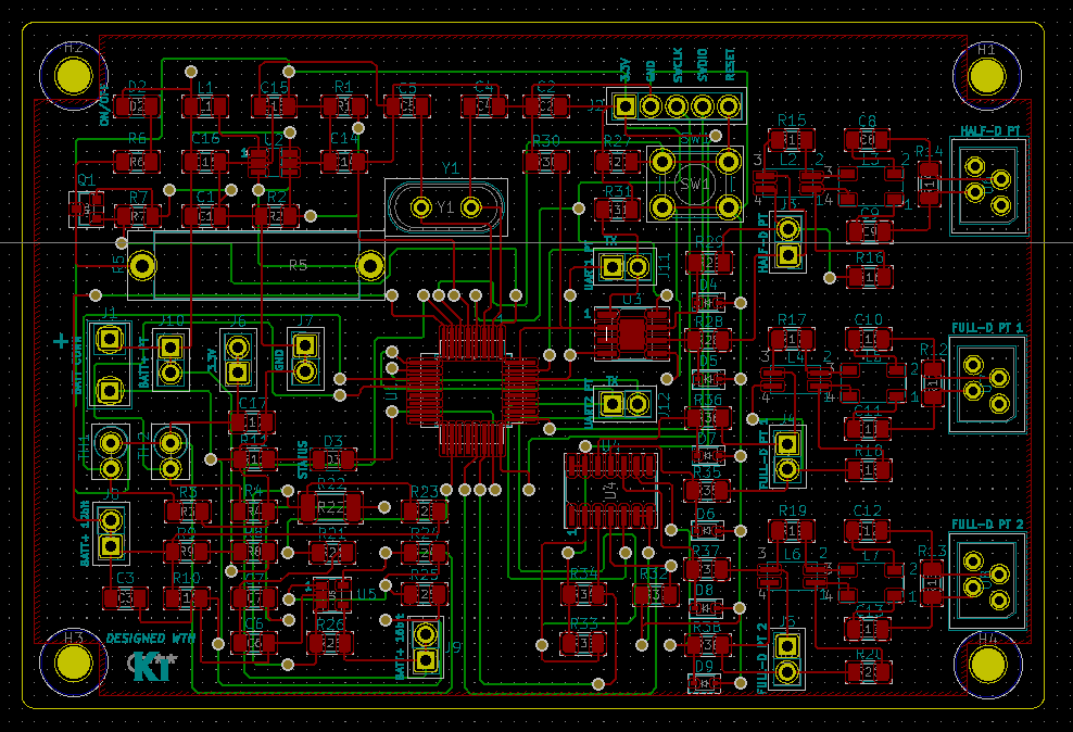
BMSv2.0 PCB Layout Design
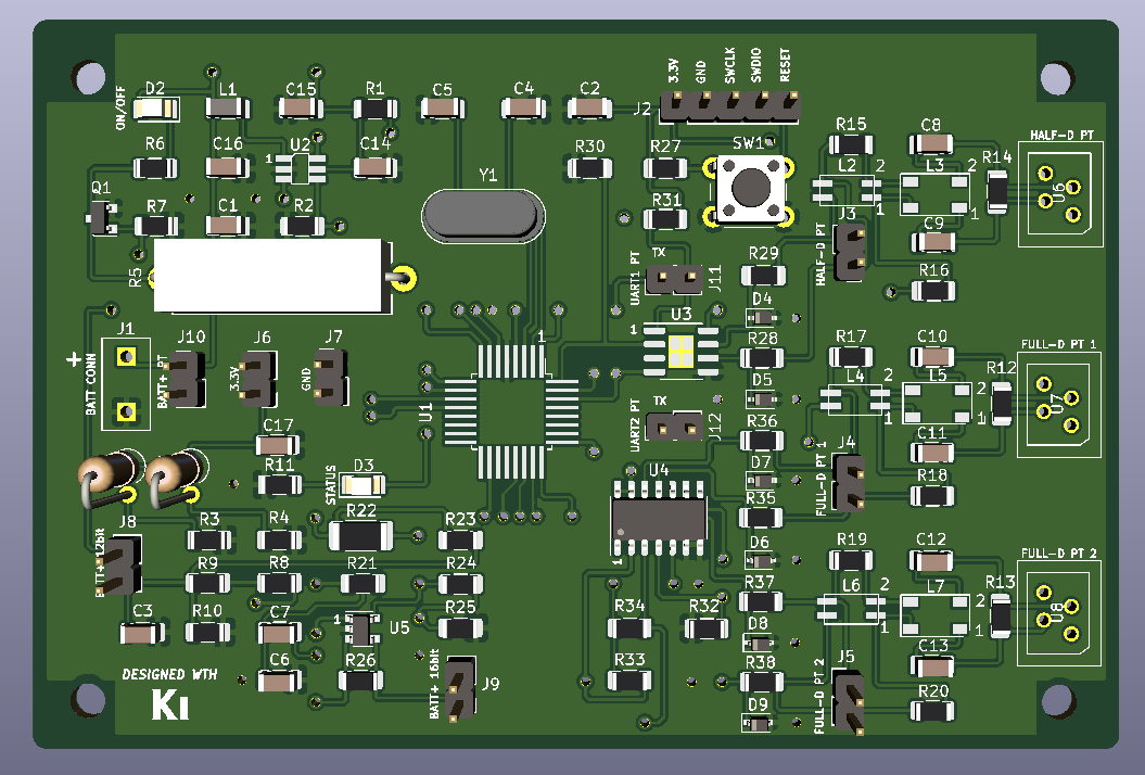
BMSv2.0 PCB 3D View
- Replace the boost converter with the buck/boost converter
- Make the hole in the footprint for communication connector header
- Replace 200k resistor with 180k resistor in the power supply block to generate correct voltage reference
- Move the cooper pour layer from the output connectors
- Put the interface to connect the board with PC
- Change PWM output pin to TIM2_CH1
- Move ADC pin from ADC1_IN1 pin (PA1) to clear the conflict with UART2 configuration
- Using FreeRTOS, one task will take analog voltage and temperature values every milisecond, another task will send the data after it gets the request

