CURRENT STATUS : stable
This is a very a simple sdram controller which works on the De0 Nano. The project also contains a simple push button interface for testing on the dev board.
Basic features
- Operates at 100Mhz, CAS 3, 32MB, 16-bit data
- On reset will go into
INITsequnce - After
INITthe controller sits inIDLEwaiting forREFRESH,READorWRITE REFRESHoperations are spaced evenly 8192 times every 32msREADis always single read with auto prechargeWRITEis always single write with auto precharge
 Host Interface          SDRAM Interface

   /-----------------------------\
   |      sdram_controller       |
==> wr_addr                  addr ==>
==> wr_data             bank_addr ==>
--> wr_enable                data <=>
   |                 clock_enable -->
==> rd_addr                  cs_n -->
--> rd_enable               ras_n -->
<== rd_data                 cas_n -->
<-- rd_ready                 we_n -->
<-- busy            data_mask_low -->
   |               data_mask_high -->
--> rst_n                        |
--> clk                          |
   \-----------------------------/
From the above diagram most signals should be pretty much self explainatory. Here are some important points for now. It will be expanded on later.
wr_addrandrd_addrare equivelant to the concatenation of{bank, row, column}rd_enableshould be set to high once an address is presented on theaddrbus and we wish to read data.wr_enableshould be set to high onceaddranddatais presented on the busbusywill go high when the read or write command is acknowledged.busywill go low when the write or read operation is complete.rd_readywill go high when datard_datais available on thedatabus.- NOTE For single reads and writes
wr_enableandrd_enableshould be set low oncebusyis observed. This will protect from the controller thinking another request is needed if left higher any longer.
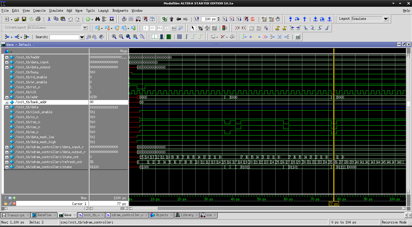
Initialization process showing:
- Precharge all banks
- 2 refresh cycles
- Mode programming
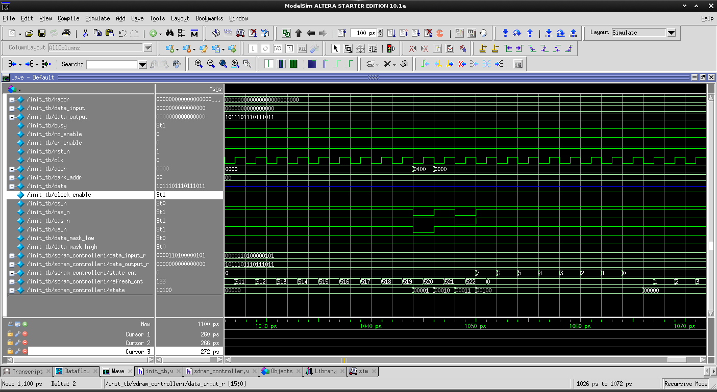
Refresh process showing:
- Precharge all banks
- Single Refresh
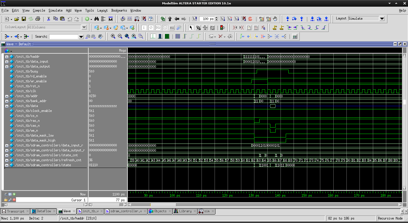
Write operation showing:
- Bank Activation & Row Address Strobe
- Column Address Strobe with Auto Precharge set and Data on bus
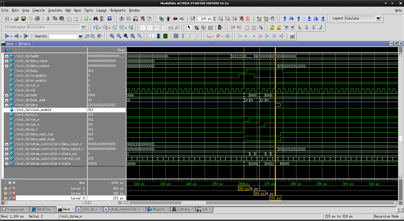
Read operation showing:
- Bank Activation & Row Address Strobe
- Column Address Strobe with Auto Precharge set
- Data on bus
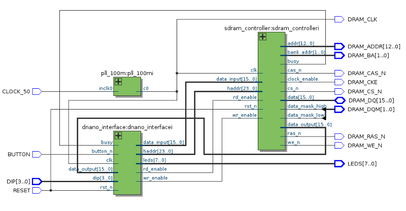 Figure - test application block diagram
The test application provides a simple user interface for testing the functionality of the sdram controller.
Basics:
- The clock input should be 50Mhz (a pll multiplies it up to 100Mhz)
- One push button is used for
reset - A Second push button is used for
readandwrite- single click for
write - double click for
read
- single click for
- A 4-bit dip switch is used for inputting addresses and data
- Upon
resetthe read/write addresses are read from the dip switch - When
writingthe dip switch is data is written to the sdram - Address and data busses are greather than 4 bits, data is duplicated to fill the bus
- Upon
- 8 LEDs are used to display the data read from the sdram. The data but is 16-bits, high and low bytes are alternated on the LEDs about every half second.
- Compiles
- Simulated
Init - Simulated
Refresh - Simulated
Read - Simulated
Write - Confirmed in De0 Nano
This project has been developed with altera quartus II.
BSD
I didn't look at these when designing my controller. But it might be good to take a look at for ideas.
- http://hamsterworks.co.nz/mediawiki/index.php/Simple_SDRAM_Controller - featured on hackaday
- http://ladybug.xs4all.nl/arlet/fpga/source/sdram.v - Arlet's implementation from a comment on the hackaday article
